Hardware Connection
Brief
More information,please reference official documents.DeveloperGuide Orin Nano/NX Core Modules (Orin Nano 4G/8G,Orin NX 8G/16G)fit to carrier board, with 260 pins SO-DIMM connector.
PCBA Interfaces
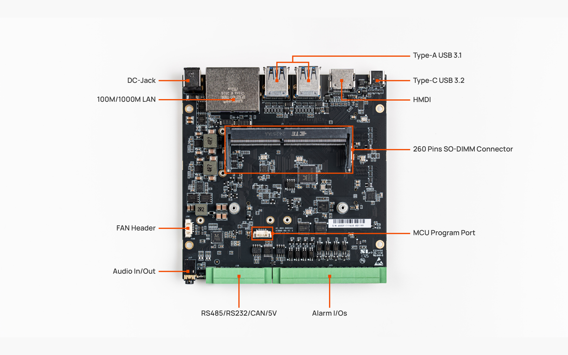
Top side Interfaces
- DC input from 12 to 36V
- 100M/1000M LAN *2
- USB Type-A *4 support USB3.1
- HDMI (Support: Orin Nano=HDMI 1.4, Orin NX=HDMI 2.1)
- USB Type-C support USB3.2
- SO-DIMM SOCKET 260 pins for Orin Nano/Nx Modules
- PWM FAN Connector
- MCU Program port
- 3.5 Phone Jack for Audio Input and Output
- Terminals for RS485, RS232, CAN, 5V Power Output
- Terminals for DI *4 and DO *4
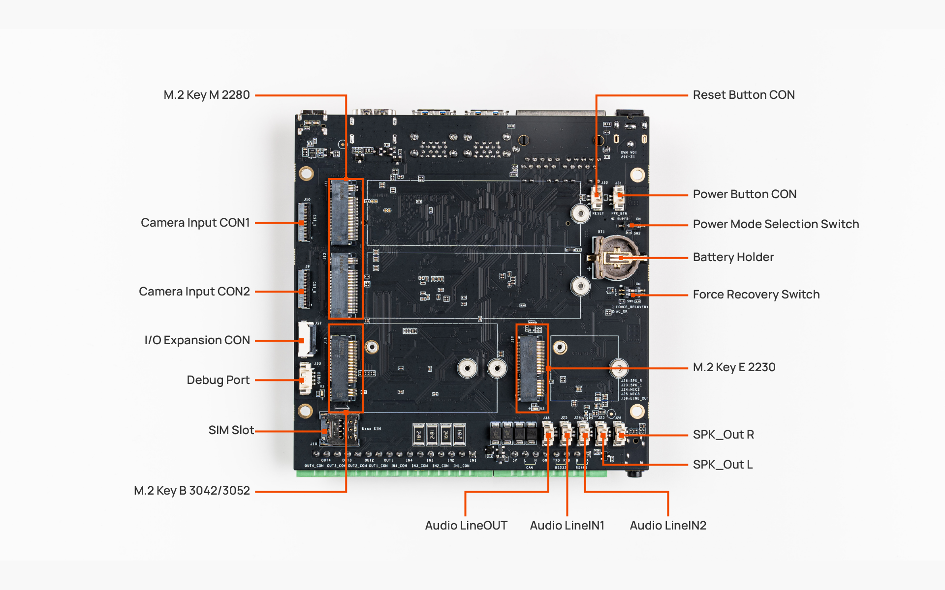
Bottom side Interfaces
- M.2 Key M 2280 for storage, support PCIe *4
- M.2 Key M 2280 for storage, support PCIe *1
- M.2 Key B 3042/3052 for Cellular,support 4G/5G Module
- M.2 Key E 2230 for WiFi&BT
- Camera Input Connector Port1, support 4 Lanes MIPI
- Camera Input Connector Port2, support 4 Lanes MIPI
- I/O Expansion Port, up to 11 GPIOs and 3.3 output
- UART Port for debug
- SIM slot
- Audio Line Output
- Audio Line Input Port1
- Audio Line Input Port2
- Audio Speaker Output L Channel
- Audio Speakper Output R Channel
- Shift switch for power mode selection
- Force Recovery Switch
- Backup Battery Holder
- Power Button Connector
- Reset Button Connector
- Power Mode Selection Switch
Quick connection guide
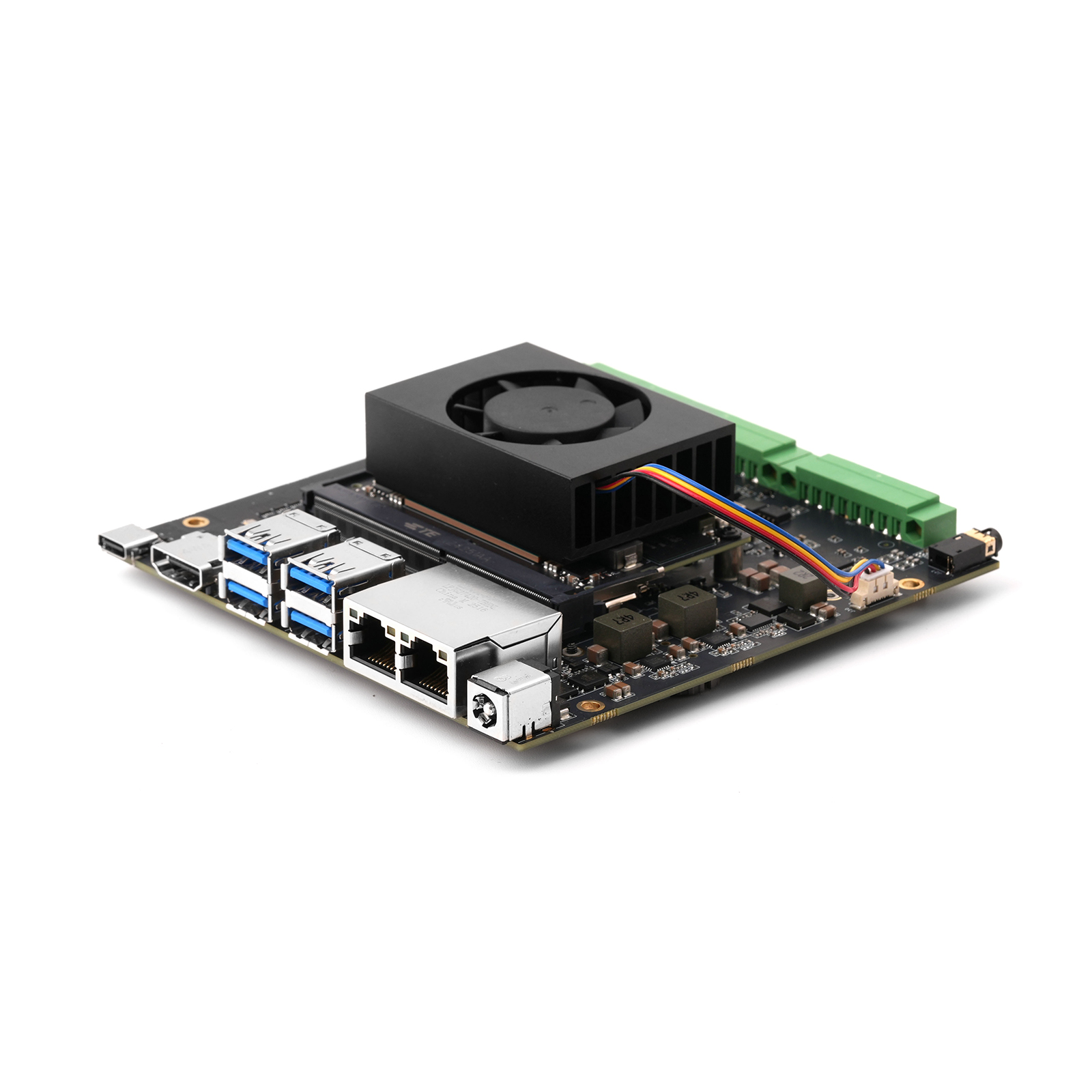
- 确认开发套件所需的清单是否齐全,包括核心模组,载板,风扇及其它周边配件
- 将风扇装配到Orin Nano/NX模组上
- 装配前确认风扇与SoC连接处理涂有导热硅脂
- 风扇散热器有器件避让槽,安装时注意和模组对齐
- 风扇固定支架方向要对,且坚固时注意不要磕坏模组上的器件
- 确认风扇用固定支架锁紧,四个固定螺丝不会松
- 将装好风扇的Orin Nano/NX模组,插扣进260 Pins SO-DIMM SOCKET,确认紧扣后,再通过两个螺比,将模组锁到Carried Board。最后风扇电子线接插到PWM FAN Connector
- 将4个支撑铜柱分别固定到四个固定孔位上,以支撑DemoKit。或将DemoKit通过外壳套件进行防护
- 翻到Carried Board 的底面,将所需的组件装配上去
- 将 RTC Battery CR1220固定到 BT1的 Holder上(Optional)
- 将SSD固定到 J11(x4 Lane) 或 J13 (x1 Lane)的M.2 Key M 2280插槽。建议系统盘装到J11,存储拓展装到J13(可选)
- 将WiFi&BT模组固定到J19的 M.2 Key E 2230(Optional)
- 将4G/5G模组固定到J15的M.2 Key B 2242, or M.2 Key B 2252 ,并将Sim卡插到J18的Sim卡槽 (Optional)
- 将树莓派镜头模组,或其它可用镜头模组连接到J9或J10 的CSI接口 (Optional)
- 若有外接按键需求,可将电源按键连接到 J31的Wafer Connector, 将复位按键连接到 J32的Wafer Connector
- 若有音频功能需求,可以将外部音源连接到 J25 , J24 Audio Line IN接口,将 J38 Audio Line Output 连接到外部音频设备,将J34, J26 Speaker Out 连接到外部喇叭,或通过音频线接入到 J27的 3.5 Audio Phone Jack 上,实现音频输入输出
- 若有其它模组或报警设备,可通过板载的Terminals 连接,包括RS485,RS232,CAN, DI,DO及外部5V供电
- 若有其它模组或报警设备,可通过 J37 FFC Connector 拓展GPIO, SPI, I2C及3V3供电,来实现外部模组的拓展
- 将调式串口工具连接到 J33的 UART2 接口
- HDMI接口连接到外部显示器
- 将有线鼠标和键标连接到USB Type-A接口中任意两个
- 将网线连接到 LAN 口中任意一个
- 将USB Type-C 接口连接到调试电脑
- 确认以上操作无误后,将电源适配器连接到 DC-JACK,即可开始进行套件开发调试
软件烧录和操作参考:System Flashing
Interfaces and instructions
There are related interafces detailed decription,which are using on the Board and product. More information please refer "Jetson Orin NX Series and Jetson Orin Nano Series Pinmux".
NVMe 协议:Non-Volatile Memory Express,是一种高性能、高并发的存储协议,专为 SSD 设计。
PCIe: (Peripheral Component Interconnect Express)是用于高速串行通信的标准接口,广泛应用于计算机内部的各种扩展卡和设备。PCIe传输通过一对差分信号线进行数据传输,每个通道包含两对差分信号线(一个用于发送,一个用于接收)。支持多通道配置,如 x1、x2、x4、x8 等,表示使用的通道数量。如M.2 Key M Port1支持x4, M.2 Key M port2支持x1。
| 特性 | Data Rate | Orin Nano | Orin NX |
|---|---|---|---|
| PCIe 3.0 | 1 GB/s @ Lane | Y | Y |
| PCIe 4.0 | 2GB/s @ Lane | X | X |
J11: M.2 Key M (4 Lanes)
此接口支持4Lanes PCIe,可用于连接SSD。
| Pin # | Signal Name | Description | Direction | Pin Type |
|---|---|---|---|---|
| 131 | PCIE0_RX0_N | PCIe 0 Receive 0– (PCIe Ctrl #4 Lane 0) | Input | PCIe PHY |
| 133 | PCIE0_RX0_P | PCIe 0 Receive 0+ (PCIe Ctrl #4 Lane 0) | Input | PCIe PHY |
| 137 | PCIE0_RX1_N | PCIe 0 Receive 1– (PCIe Ctrl #4 Lane 1) | Input | PCIe PHY |
| 139 | PCIE0_RX1_P | PCIe 0 Receive 1+ (PCIe Ctrl #4 Lane 1) | Input | PCIe PHY |
| 149 | PCIE0_RX2_N | PCIe 0 Receive 2– (PCIe Ctrl #4 Lane 2) | Input | PCIe PHY |
| 151 | PCIE0_RX2_P | PCIe 0 Receive 2+ (PCIe Ctrl #4 Lane 2) | Input | PCIe PHY |
| 155 | PCIE0_RX3_N | PCIe 0 Receive 3– (PCIe Ctrl #4 Lane 3) | Input | PCIe PHY |
| 157 | PCIE0_RX3_P | PCIe 0 Receive 3+ (PCIe Ctrl #4 Lane 3) | Input | PCIe PHY |
| 134 | PCIE0_TX0_N | PCIe 0 Transmit 0– (PCIe Ctrl #4 Lane 0) | Output | PCIe PHY |
| 136 | PCIE0_TX0_P | PCIe 0 Transmit 0+ (PCIe Ctrl #4 Lane 0) | Output | PCIe PHY |
| 140 | PCIE0_TX1_N | PCIe 0 Transmit 1– PCIe Ctrl #4 Lane 1) | Output | PCIe PHY |
| 142 | PCIE0_TX1_P | PCIe 0 Transmit 1+ (PCIe Ctrl #4 Lane 1) | Output | PCIe PHY |
| 148 | PCIE0_TX2_N | PCIe 0 Transmit 2– (PCIe Ctrl #4 Lane 2) | Output | PCIe PHY |
| 150 | PCIE0_TX2_P | PCIe 0 Transmit 2+ (PCIe Ctrl #4 Lane 2) | Output | PCIe PHY |
| 154 | PCIE0_TX3_N | PCIe 0 Transmit 3– (PCIe Ctrl #4 Lane 3) | Output | PCIe PHY |
| 156 | PCIE0_TX3_P | PCIe 0 Transmit 3+ (PCIe Ctrl #4 Lane 3) | Output | PCIe PHY |
| 181 | PCIE0_RST* | PCIe 0 Reset (PCIe Ctrl #4) | Bidir | Open Drain 3.3V |
| 180 | PCIE0_CLKREQ* | PCIE 0 Clock Request (PCIe Ctrl #4) | Bidir | Open Drain 3.3V |
| 179 | PCIE_WAKE* | PCIe Wake | Bidir | Open Drain 3.3V |
| 160 | PCIE0_CLK_N | PCIe #0 Reference Clock- | Bidir | PCIe PHY |
| 162 | PCIE0_CLK_P | PCIe #0 Reference Clock+ | Bidir | PCIe PHY |
| 232 | I2C2_SCL | General I2C 2 Clock | Bidir | Open Drain – 1.8V |
| 234 | I2C2_SDA | General I2C 2 Data | Bidir | Open Drain – 1.8V |
J12: M.2 Key M (1 Lanes)
此接口支持1Lanes PCIe,可用于连接SSD。
| Pin # | Signal Name | Description | Direction | Pin Type |
|---|---|---|---|---|
| 40 | PCIE2_RX0_N | PCIe 2 Receive 0– (PCIe Ctrl #7 Lane 0) | Input | PCIe PHY |
| 42 | PCIE2_RX0_P | PCIe 2 Receive 0+ (PCIe Ctrl #7 Lane 0) | Input | PCIe PHY |
| 46 | PCIE2_TX0_N | PCIe 2 Transmit 0– (PCIe Ctrl #7 Lane 0) | Output | PCIe PHY |
| 48 | PCIE2_TX0_P | PCIe 2 Transmit 0+ (PCIe Ctrl #7 Lane 0) | Output | PCIe PHY |
| 52 | PCIE2_CLK_N | PCIe 2 Reference Clock– (PCIe Ctrl #7) | Output | PCIe PHY |
| 54 | PCIE2_CLK_P | PCIe 2 Reference Clock+ (PCIe Ctrl #7) | Output | PCIe PHY |
| 179 | PCIE_WAKE* | PCIe Wake | Bidir | Open Drain 3.3V |
| 219 | PCIE2_RST* | PCIe 2 Reset (PCIe Ctrl #7) | Output | PCIe PHY |
| 221 | PCIE2_CLKREQ* | PCIe 2 Clock Request (PCIe Ctrl #7) | Bidir | PCIe PHY |
| 232 | I2C2_SCL | General I2C 2 Clock | Bidir | Open Drain – 1.8V |
| 234 | I2C2_SDA | General I2C 2 Data | Bidir | Open Drain – 1.8V |
J15: M.2 Key B
此接口用于连接4G/5G模组。
| Pin # | Signal Name | Description | Direction | Pin Type |
|---|---|---|---|---|
| / | USB2_HUB2_P | from usb hub | Bidir | |
| / | USB2_HUB2_N | from usb hub | Bidir | |
| 51 | USBSS2_RX_N | USB SS Receive– (USB 3.2 Ctrl #2) | Input | USB SS PHY |
| 53 | USBSS2_RX_P | USB SS Receive+ (USB 3.2 Ctrl #2) | Input | USB SS PHY |
| 57 | USBSS2_TX_N | USB SS Transmit– (USB 3.2 Ctrl #2) | Output | USB SS PHY |
| 59 | USBSS2_TX_P | USB SS Transmit+ (USB 3.2 Ctrl #2) | Output | USB SS PHY |
| 118 | GPIO01 | WWAN_PWR_ON_N | Input | CMOS – 1.8V |
| 97 | SPI0_CS1* | WWAN_WAKE_EN | Bidir | CMOS – 1.8V |
| 91 | SPI0_SCK | SPI 0 Clock | Bidir | CMOS – 1.8V |
| 89 | SPI0_MOSI | SPI 0 Master Out / Slave In | Bidir | CMOS – 1.8V |
| 93 | SPI0_MISO | SPI 0 Master In / Slave Out | Bidir | CMOS – 1.8V |
| 95 | SPI0_CS0* | SPI 0 Chip Select 0 | Bidir | CMOS – 1.8V |
| 126 | GPIO01 | M2B_RST_N | Input | CMOS – 1.8V |
| / | USIM_RST | Connect to Sim Card for reset | Output | |
| / | USIM_CLK | Connect to Sim Card for clock | Output | |
| / | USIM_DATA | Connect to Sim Card for Data | Bidir | |
| / | USIM_PWR | Connect to Sim Card for power supply | Power | |
| / | USIM_DET | Connect to Sim Card for card detection | Input |
J19: M.2 Key E
此接口用于连接WiFi/BT模组
| Pin # | Signal Name | Description | Direction | Pin Type |
|---|---|---|---|---|
| / | USB2_HUB1_P | from usb hub | Bidir | |
| / | USB2_HUB1_N | from usb hub | Bidir | |
| 167 | PCIE1_RX0_N | PCIe 1 Receive 0– (PCIe Ctrl # 1 Lane 0) | Input | PCIe PHY |
| 169 | PCIE1_RX0_P | PCIe 1 Receive 0+ (PCIe Ctrl # 1 Lane 0) | Input | PCIe PHY |
| 172 | PCIE1_TX0_N | PCIe 1 Transmit 0– (PCIe Ctrl # 1 Lane 0) | Output | PCIe PHY |
| 174 | PCIE1_TX0_P | PCIe 1 Transmit 0+ (PCIe Ctrl # 1 Lane 0) | Output | PCIe PHY |
| 173 | PCIE1_CLK_N | PCIe 1 Reference Clock– (PCIe Ctrl #1) | Output | PCIe PHY |
| 175 | PCIE1_CLK_P | PCIe 1 Reference Clock+ (PCIe Ctrl #1) | Output | PCIe PHY |
| 179 | PCIE_WAKE* | PCIe Wake. 47kΩ pull-up to 3.3V on the module. | Bidir | Open Drain 3.3V |
| 182 | PCIE1_CLKREQ* | PCIe 1 Clock Request (PCIe Ctrl # 1). 47kΩ pull-up to 3.3V on the module | Bidir | PCIe PHY |
| 183 | PCIE1_RST* | PCIe 1 Reset (PCIe Ctrl #1). 4.7kΩ pull-up to 3.3V on the module | Output | PCIe PHY |
| 232 | I2C2_SCL | General I2C 2 Clock | Bidir | Open Drain – 1.8V |
| 234 | I2C2_SDA | General I2C 2 Data | Bidir | Open Drain – 1.8V |
| 128 | GPIO05 | Wifi disable control | Output | CMOS – 1.8V |
| 210 | CLK_32K_OUT | M2E_SubClk_32KHz | Output | Clk Soure |
J9: Camera Interface
此接口为CSI0支持4lanes MIPI,用于连接Camera Module。
| Pin # | Signal Name | Description | Direction | Pin Type |
|---|---|---|---|---|
| 4 | CSI0_D0_N | Camera, CSI 0 Data 0– | Input | MIPI D-PHY |
| 6 | CSI0_D0_P | Camera, CSI 0 Data 0+ | Input | MIPI D-PHY |
| 16 | CSI0_D1_N | Camera, CSI 0 Data 1– | Input | MIPI D-PHY |
| 18 | CSI0_D1_P | Camera, CSI 0 Data 1+ | Input | MIPI D-PHY |
| 10 | CSI0_CLK_N | Camera, CSI 0 Clock– | Input | MIPI D-PHY |
| 12 | CSI0_CLK_P | Camera, CSI 0 Clock+ | Input | MIPI D-PHY |
| 3 | CSI1_D0_N | Camera, CSI 1 Data 0– | Input | MIPI D-PHY |
| 5 | CSI1_D0_P | Camera, CSI 1 Data 0+ | Input | MIPI D-PHY |
| 15 | CSI1_D1_N | Camera, CSI 1 Data 1– | Input | MIPI D-PHY |
| 17 | CSI1_D1_P | Camera, CSI 1 Data 1+ | Input | MIPI D-PHY |
| 114 | CAM0_PWDN | Camera 0 Powerdown or GPIO | Bidir | CMOS – 1.8V |
| 116 | CAM0_MCLK | Camera 0 Reference Clock | Bidir | CMOS – 1.8V |
| 213 | CAM_I2C_SCL | Camera I2C Clock. 2.2kΩ pull-up to 3.3V on the module. | Bidir | Open Drain – 3.3V |
| 215 | CAM_I2C_SDA | Camera I2C Data. 2.2kΩ pull-up to 3.3V on the module. | Bidir | Open Drain – 3.3V |
| 130 | GPIO06 | I2C Channel selection, Low for CSI0 | Output | CMOS – 1.8V |
J10: Camera Interface
此接口为CSI1支持4lanes MIPI,用于连接Camera Module。
| Pin # | Signal Name | Description | Direction | Pin Type |
|---|---|---|---|---|
| 24 | CSI2_D0_P | Camera, CSI 2 Data 0+ | Input | MIPI D-PHY |
| 34 | CSI2_D1_N | Camera, CSI 2 Data 1– | Input | MIPI D-PHY |
| 36 | CSI2_D1_P | Camera, CSI 2 Data 1+ | Input | MIPI D-PHY |
| 28 | CSI2_CLK_N | Camera, CSI 2 Clock– | Input | MIPI D-PHY |
| 30 | CSI2_CLK_P | Camera, CSI 2 Clock+ | Input | MIPI D-PHY |
| 21 | CSI3_D0_N | Camera, CSI 3 Data 0– | Input | MIPI D-PHY |
| 23 | CSI3_D0_P | Camera, CSI 3 Data 0+ | Input | MIPI D-PHY |
| 33 | CSI3_D1_N | Camera, CSI 3 Data 1– | Input | MIPI D-PHY |
| 35 | CSI3_D1_P | Camera, CSI 3 Data 1+ | Input | MIPI D-PHY |
| 120 | CAM1_PWDN | Camera 1 Powerdown or GPIO | Bidir | CMOS – 1.8V |
| 122 | CAM1_MCLK | Camera 1 Reference Clock | Bidir | CMOS – 1.8V |
| 213 | CAM_I2C_SCL | Camera I2C Clock. 2.2kΩ pull-up to 3.3V on the module. | Bidir | Open Drain – 3.3V |
| 215 | CAM_I2C_SDA | Camera I2C Data. 2.2kΩ pull-up to 3.3V on the module. | Bidir | Open Drain – 3.3V |
| 130 | GPIO06 | I2C Channel selection, High for CSI1 | Output | CMOS – 1.8V |
Audio Interface
| Interfaces | Functions | Descriptions |
|---|---|---|
| J27 | 3.5 Audio Phone Jack | Support Audio Output and Mic Input |
| J24 | Mic Input | Mono Audio Output or Mic Input, Pin1=In/Out,Pin2=GND |
| J25 | Mic Input | Mono Audio IOutput or Mic Input, Pin1=In/Out,Pin2=GND |
| J23 | Speaker Output | Right Channel differential output: Pin1=Positive, Pin2=Negative |
| j26 | Speaker Output | Left Channel differential output: Pin1=Positive, Pin2=Negative |
| J38 | Line Output | L/R Chanel Line Output: Pin1=Left, Pin2=Right |
14 Pins Expansion IOs
此接口可以配拓展板来连接外围设备。
| Pin # | Signal Name | Description | Direction | Pin Type |
|---|---|---|---|---|
| 103 | UART0_RTS* | UART #0 Request to Send | Output | CMOS – 3.3V |
| 105 | UART0_CTS* | UART #0 Clear to Send | Input | CMOS – 3.3V |
| / | GND | GND | GND | GND |
| 106 | SPI1_SCK | SPI 1 Clock | Bidir | CMOS – 3.3V |
| 108 | SPI1_MISO | SPI 1 Master In / Slave Out | Bidir | CMOS – 3.3V |
| 104 | SPI1_MOSI | SPI 1 Master Out / Slave In | Bidir | CMOS – 3.3V |
| 110 | SPI1_CS0* | SPI 1 Chip Select 0 | Bidir | CMOS – 3.3V |
| 112 | SPI1_CS1* | SPI 1 Chip Select 1 | Bidir | CMOS – 3.3V |
| 189 | I2C1_SCL | General I2C 1 Clock. 2.2kΩ pull-up to 3.3V on the module. | Bidir | Open Drain – 3.3V |
| 191 | I2C1_SDA | General I2C 1 Data. 2.2kΩ pull-up to 3.3V on the module. | Bidir | Open Drain – 3.3V |
| 185 | I2C0_SCL | General I2C 0 Clock. 1.5kΩ pull-up to 3.3V on module. | Bidir | Open Drain – 3.3V |
| 187 | I2C0_SDA | General I2C 0 Data. 1.5kΩ pull-up to 3.3V on the module. | Bidir | Open Drain – 3.3V |
| / | GND | GND | / | GND |
| / | 3.3V | Power Supply 3.3V with fuse | Output | 3.3V |
Note:
- I2C0 also connect to Type-C USB control and TPM
- CMOS type IOs have been translate to 3.3V from 1.8V
Rear panel expansion IOs
Please note that the Alarm IOs are dry contact.
| Pin # | Signal Name | Description | Direction | Pin Type |
|---|---|---|---|---|
| 218 | GPIO12 | GPIO=Low/high when IN1=high(Open)/low(Short) | Input | dry contact |
| IN1_COM: COM pin | ||||
| 216 | GPIO11 | IN2: GPIO=Low/high when IN1=high(Open)/low(Short) | Input | dry contact |
| IN2_COM: COM pin | ||||
| 206 | GPIO07 | IN3: GPIO=Low/high when IN1=high(Open)/low(Short) | Input | dry contact |
| IN3_COM: COM pin | ||||
| 228 | GPIO13 | IN4: GPIO=Low/high when IN1=high(Open)/low(Short) | Input | dry contact |
| IN4_COM: COM pin | ||||
| 199 | I2S0_SCLK_1V8 | OUT1: GPIO=Low for short, high for open | Output | dry contact |
| OUT1_COM: COM pin | ||||
| 197 | I2S0_LRCK_1V8 | OUT2: GPIO=Low for short, high for open | Output | dry contact |
| OUT2_COM: COM pin | ||||
| 195 | I2S0_SDIN_1V8 | OUT3: GPIO=Low for shor, high for open. | Output | dry contact |
| OUT3_COM: COM pin | ||||
| 193 | I2S0_SDOUT_1V8 | OUT4: GPIO=Low for short, high for open. | Output | dry contact |
| OUT4_COM: COM pin |
| Pin # | Signal Name | Description | Direction | Pin Type |
|---|---|---|---|---|
| 203 | UART1_TXD | Use for RS_485 | Output | CMOS 1.8V |
| 205 | UART1_RXD | Use for RS_485 | Input | CMOS 1.8V |
| 207 | UART1_RTS* | RS_485 enable pin | Output | CMOS 1.8V |
| 99 | UART0_TXD | Use for uart Ransmit (with 3.3 level shifter) | Output | CMOS – 1.8V |
| 101 | UART0_RXD | Use for uart Receive (with 3.3 level shifter) | Input | CMOS – 1.8V |
| / | GND | GND | GND | GND |
| 145 | CAN_TX | FD CAN Transmit | Output | CMOS – 3.3V |
| 143 | CAN_RX | FD CAN Receive | Input | CMOS – 3.3V |
| / | VCC_5V | VCC_5V | Output | 5V |